
Chip Innovator
Custom Semiconductor Packaging & Testing
Chip Innovator supports the transition from bare die to packaged devices through custom package design, manufacturing and testing for legacy parts and new designs.
Discuss Packaging & Testing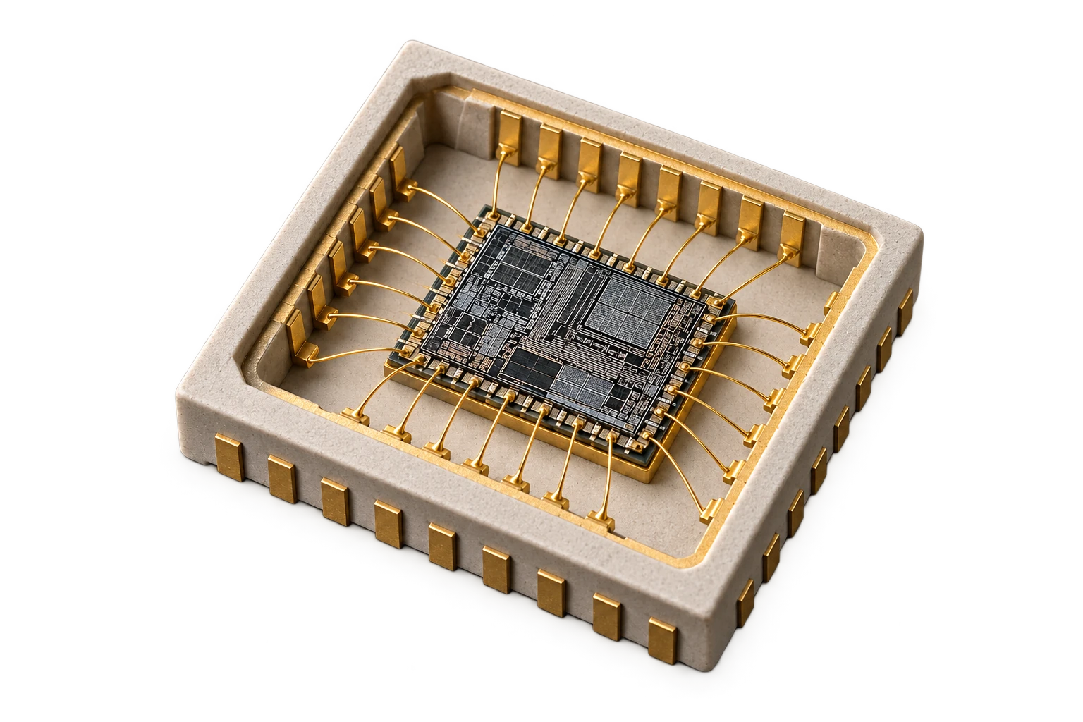
Custom package design and manufacturing
Share the selected die, target package dimensions, footprint, connections and operating conditions. Our engineering team reviews the package requirements and coordinates a solution for your application, using material from our inventory or global sourcing network where appropriate.
Legacy package recreation
For continued production of an existing design, provide the original device dimensions, pin configuration and application requirements. The scope of recreation and any differences from the original device require project-specific engineering review.
Electrical and reliability testing
Test programmes are defined around your device specifications and acceptance requirements. Discuss electrical and functional checks, burn-in, reliability screening and environmental testing with our team. The test scope, conditions and reporting are agreed for each project.
Prepare your project enquiry
Include a datasheet, package drawing if available, required quantity, operating temperature range and the tests or qualification requirements you need. Tell us in your enquiry message if you need a datasheet or other documents before defining the project.
Contact Chip Innovator at sales@chipinnovator.com, or send your project requirements.